TRACE – Automating Hardware Teardowns
In our last blog post, we touched upon an internal tool we created called TRACE (Teardown Recognition and Analysis of Component Elements). TRACE scans Printed Circuit Boards (PCBs) to capture an ultra high-resolution view of the board to aid in hardware reverse engineering. In this post we’ll provide a full breakdown of how, and why, it was made.
The problem
TRACE started with a fairly simple problem: reverse engineering PCBs is often a slow and repetitive process which takes up valuable research time. Before you can even begin understanding how a circuit works, there’s usually a lot of groundwork to do, identifying components, reading tiny package markings, finding datasheets, tracing power rails, identifying debug ports and generally figuring out what you’re looking at.
The goal of this project wasn’t to automate reverse engineering or replace the engineer, which has been shown to be a fool’s errand. Instead, it was to automate the repetitive parts of the process so that more time could be spent on the interesting bits such as understanding how the hardware works, diagnosing faults, or figuring out why a design behaves the way it does.
It also became a good excuse to experiment with some newer AI vision models. Rather than asking them to solve the entire problem in one go, the idea was to use them where they actually add value providing context for a board, reading package markings, and speeding up component identification while leaving the engineering decisions to the person using the tool. Also… we thought it would also be really cool to get a high resolution image of the PCBs we are working on!
The Hardware
At CoreTech, we provide researchers and engineers the opportunity to work on innovation projects. These are designed to use technology to improve upon something or make our lives easier, separately from our client-work. As such, our first step was to review the hardware options around our innovation budget, and create a number of goals we wanted to achieve in bringing our idea to life. These were:
-
Repurpose one of our old 3D printers which wasn’t in use
-
Mount camera and lighting equipment
-
Provide the ability to manually focus
-
Provide the ability to set light locations and brightness
-
-
Be able to manually control the movements via GCODE commands
-
Control the hardware via a simple graphical user interface
Ender 3 Repurposed
An Ender 3 3D printer was discovered to be a good candidate as the hot end could be easily replaced, with measurements/CAD models being openly available online. This helped when it came to the design phase around mounting the camera and making custom CAD models.
Sections of the printer needed to be stripped down to make way for our modifications, this included; the extruder, sensors (for example, replacing a bltouch auto-leveling sensor in a form of an end stop), hot bed plate, and manual levelling system.
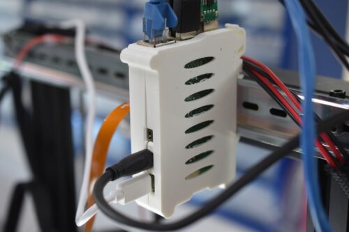
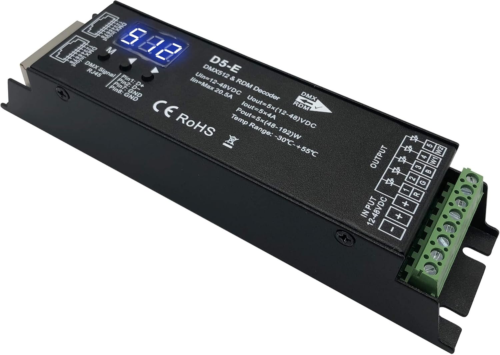
At the top of the Ender 3, a DIN mounting plate was fixed onto the 2020 aluminium scaffolding to enable a series of equipment to be mounted. This included the 5 channel DMX controller and a Raspberry Pi 5. Power was taken from the 24V output on the power supply, with buckdown modules used wherever a lower voltage was required.
Translation and Image Capturing Software
On the Raspberry Pi 5, we created a custom service that enabled the following features.
- Providing a method to take input from the client GUI in the form of:
- a definition of the minimum/maximum x,y coordinates to photograph;
- project details to help with file/directory naming.
- Enabling light control to be switched on/off or set to a dimmable value
- Interacting with the camera to take photos per moment
This enabled the setup to have an automated approach to capturing every aspect of a PCB without requiring manual photos. We wrote the service in Python and wrapped it in a Docker container to enable the system to be integrated to other devices in the future.
Control Software
We started by looking into Marlin as the main control software before quickly realising that a significant refactor would be required to strip out the detection code for the sensors that were removed. Rather than going down that route we switched to using Klipper which provides a much more flexible configuration, allowing us to create a custom system without having to trawl through lines and lines of code.
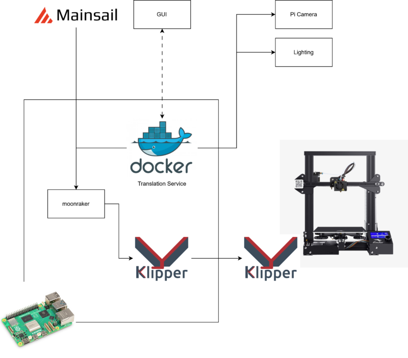
Once the Klipper firmware was setup on both pieces of hardware, control MCU and the Raspberry Pi 5, we were able to focus on issuing commands to the Ender Klipper firmware. The Klipper ecosystem has a range of packages that enable fine control over operations, from sending a command to seeing an overview GUI interface. For TRACE, we only really needed the Mainsail and Moonraker services. Mainsail provides a web-based GUI to monitor and control your hardware, making it useful to debug any issues. Moonraker (aside from being the title of a bonkers 1979 Bond film), facilitates the communication between front and back end, exposing a port that the client can interact with and redirecting commands to the Klipper service.
In between the Moonraker and Klipper API, is our own Python Flask translation service that services client requests from the main GUI software we created, running on another host, with the flow shown in the diagram below.
Camera Setup
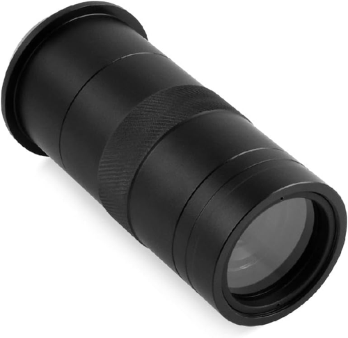
The camera sensor that we chose to use was the Raspberry Pi High Quality Camera with an inexpensive 100X microscope lens attached via the mounting point.
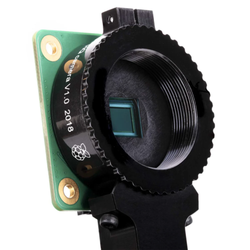
The lens focal wheel, as seen in the next section, was modified to attach gear cogs to enable the ability for a servo to focus the lens via GCODE.
3D Printed Parts
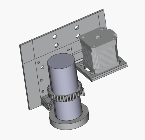
We found that we needed to develop a custom bracket to hold the camera and servo for focus with the intention of attaching onto the Ender 3 belt via the pre-existing gantry mounting plate holes. Here’s the design:
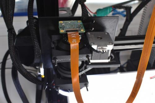
Followed by the result.
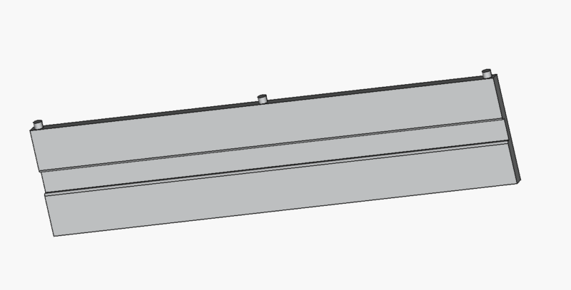
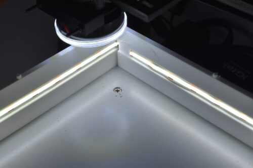
Lighting panels were also created to host the LED strips and mount onto the original aluminium gantry plate. The pegs that you can see on the edge of the panels were added to enable stacking of the LED strips if required.
Lighting
On the subject of lighting, five sets of lights, that can be dimmed if required, were installed and attached to a DMX controller (a digital lighting system allowing precise control of colour, intensity and other parameters of LED lights). A USB module, which supports the DMX protocol over RS485, was attached to the Raspberry Pi 5 to send communication to the controller. This enables the user to be able to set the best light conditions for each PCB under review.
When all this was put together we had a highly controllable environment for the photography.
Networking
To enable the user to collect the photos captured by the device we decided upon a simple SMB service. This provided a way to off-load the processing from the main Raspberry Pi 5, to enable its sole purpose to be conducting the high-res captures.
Hardware Output
Admittedly, the completed hardware rig looks rather messy. That being said it performs the job for which it was designed admirably. The system can perform automated image capturing of a PCB without manual intervention, leaving the user free to work on other tasks.
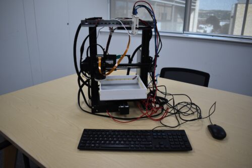
Image Capture
With the hardware connected, everything is controlled through a single GUI that handles camera movement, focus, lighting and image capture with a stream from the camera showing a live view.
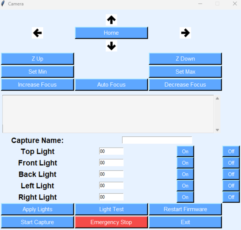
The camera is moved to opposite corners of the board to set the minimum and maximum X/Y coordinates, which defines the area that needs to be photographed.
Next comes focus and lighting. The camera height and focus level on the lens is set until the component markings and PCB traces are in sharp focus, after which the LED brightness can be adjusted from 0 to 255 to reduce glare and improve the visibility of faint text.
Once everything looks correct, the capture starts. The 3D printer moves the camera across the defined area in a grid, taking a series of overlapping close-up photographs. These images are then stitched together into one large, detailed view of the PCB, ready to be marked up and analysed. An example of an ESP32 dev board is shown below, made up of around 300 images. Note that the image size has been reduced significantly for this blog.
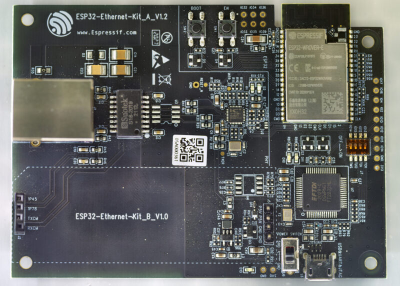
Image Annotation
Once the image has been captured, the first thing we usually want to do is start pointing at things and asking, “What’s that?”. So annotating the image is the next logical step.
Using TRACE, you can draw bounding boxes around anything that catches your eye, a mystery IC, a connector, a regulator, or even a whole section of the board. Every box gets a number automatically, and you can add notes alongside it. The size and colour of all bounding boxes can be modified within the software. We found this much nicer than scribbling on screenshots or trying to remember which component was looked at twenty minutes ago. You can also add symbols and textual data onto the image itself.
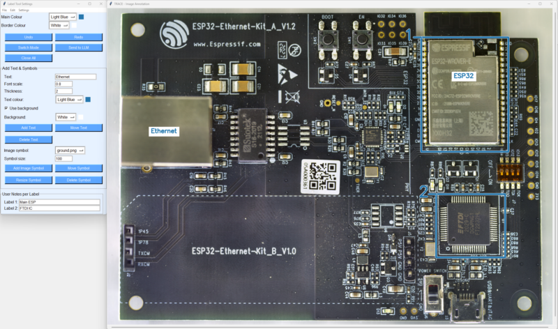
Before looking at any individual components, the entire board is sent to a vision enabled LLM. The idea here isn’t to identify every resistor or capacitor, but to get the bigger picture. It looks for clues about the board’s purpose, identifies the main functional blocks, spots likely power supplies and voltage regulators, highlights connectors and debug interfaces such as JTAG or UART, and generally tries to answer the question, “What am I looking at?”
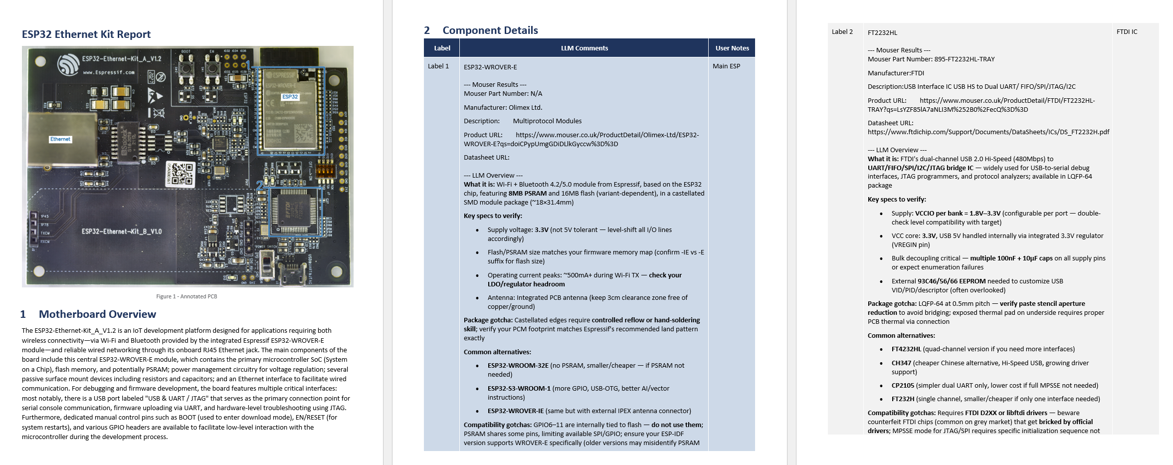
Once that’s done, the focus shifts to the annotations. Each marked region is cropped into its own image and sent to the LLM individually. Rather than asking it to reverse engineer the circuit, the prompt is deliberately narrow: read the markings on the package and tell me the part number. Breaking the problem down into dozens of small, focused tasks turned out to work much better than asking one enormous question about the whole board. It is then asked for the purpose of the component.
If the model manages to extract a part number, the software then heads off to a common component supplier website, Mouser, to see what it can find. If there’s a match, back comes the datasheet, manufacturer information, package type, and a description of the component. It’s essentially automating the part of reverse engineering where you spend half your afternoon opening browser tabs and searching for tiny strings of text printed on ICs. It then produces a report containing all this information as well as the annotated image in our internal template.
None of this replaces actually understanding the hardware. The LLM gets things wrong from time to time, especially if the markings are faint or obscured. But even when it’s not perfect, it does a good job of speeding up the repetitive parts of the process, looking up components, finding datasheets, and giving you a solid starting point.
Future Improvements
One obvious limitation at the moment is image capture. The system currently photographs the PCB at a single focus distance, which works well for reasonably flat boards but starts to struggle with taller components or uneven PCBs. A future improvement is to capture multiple images at different focus depths and combine them using focus stacking, producing a single image that’s sharp across the entire board.
Another one is that the size of the Ender 3 bed limits the PCBs we can capture to small-medium sized. One way we wanted to improve this in the future is to upgrade to an Ender 5, which has a much bigger bed size.
This post was written by Dale and Aneesh, who are both members of CoreTech’s Operational Research team.
Do you have an endless curiosity for technology?
Get ready to work with some of the most brilliant minds who care more about solving problems than climbing hierarchies.